MHz Crystal Oscillator
FCXO-05W
2.5 × 2.0 (mm: L × W)


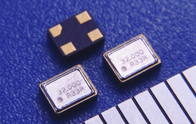
2520size MHz Crystal Oscillator (105℃ type)
- 1 ~ 80 MHz CMOS crystal clock oscillator : wide operating temperature range of -40 ~ +105℃available
- Frequency tolerance of ±7 ppm (@25℃) available
- Robust ceramic package with metal lid sealed by electron beam
- Specifications in conformity with AEC-Q200 available on request
USE
-
 Smartphone
-
 Automotive
-
 Wireless
communications
/ IoT -
 Audiovisual
equipment -
 Medical
/ Healthcare
SPECIFICATION
-
Length
2.5mm -
Width
2.0mm -
Height
0.90mm,Max -
Nominal
1〜80MHz
frequency -
Operating
-40〜105℃
temperature
| Item | Specifications | ||||
|---|---|---|---|---|---|
| Nominal frequency (MHz) | 1.000 〜 80.000 | ||||
| Frequency tolerance (ppm) (@ 25 ℃) |
±7, ±10, ±15, ±20, ±30, ±50, O.A, other | ||||
| Storage temperature (℃) (Not applicable to packaging materials) |
−55 〜 +125, other | ||||
| Operating temperature (℃) | −20 〜 +70 | −30 〜 +85 | −40 〜 +85 | −40 〜 +105 | Other combinations |
| Frequency temperature characteristics (ppm) (Refer to 25 ℃) |
±10 ±15 ±20 ±30 ±50 |
±10 ±15 ±20 ±30 ±50 |
±15 ±20 ±30 ±50 |
±30 ±50 |
|
swipe
| Item | Specifications | Conditions / Remarks | |
|---|---|---|---|
| Supply voltage, VDD (V) | +1.6 〜 +3.63 | ||
| Current consumption (mA) | 3.0 Max. | F = 40 MHz, VDD = 3.0 V, No load | |
| Stand-by current (µA) | 10 Max. | Stand-by = “L” | |
| Output voltage, VOH (V) | VDD 0.9 Min. | IOH = −4 mA | |
| Output voltage, VOL (V) | 0.1 Max. | IOL = +4 mA | |
| Output load (pF) | 15 Max. | ||
| Output level | CMOS | ||
| Symmetry (Duty Cycle) (%) | 50 ± 5 | ||
| Rise time (ns)/ Fall time (ns) | 5.0 Max. | 10 % VDD to 90 % VDD level | |
| Start-up time (ms) | 2.0 Max. | VDD = 3.3 V | |
| 5.0 Max. | VDD = 1.8 V | ||
| Random Jitter, RJ (ps) *1 | 3.7 Typ. | VDD = 3.3 V | |
| Total Jitter, TJ (ps) *1 | 51 Typ. | VDD = 3.3 V, TJ = n × RJ n ≒ 14.1, BER = 10-12) |
|
| Phase Jitter (ps) | 1.0 Max. | VDD = 3.3 V Offset frequency: 12 kHz 〜 5 MHz |
|
| Stand-by function (Pin #1) (V) | (High) | 0.7VDD Min. | Output (Pin #3) enabled |
| (Low) | 0.3VDD Max. | Output (Pin #3) disabled = High-Z | |
| Tape and reel (pcs/reel) (Reel diameter: Φ180 mm) |
3000 Max. | ||
swipe
*1 Measured on Wave Crest 3100C
Questions, business meetings, etc.
Please contact us with any queries.
Please contact us with any queries.